EME223 630m Band Transverter
- EME223-630M Description:
Updated! June22
- Kit Constructors Alert:
Updated! Jan26 - EME223-630M Rev1.x Kit Notes:
Updated! July24 - EME223-630M Rev2.x Kit Notes:
Updated! Feb25 - EME223-630M Kit Performance Tests:
- Mounting into an Enclosure:
- Antennas and Operation:
- Kit Changes and Updates:
Updated! July24
- Buy A EME223-630M Kit:
- MF 472kHz 630m Band Information Links:
The complete high performance 472 to 479kHz ( 630m Band ) Transverter Kit makes it very easy to get onto the 630m band especially with weak signal digital modes, but being linear it will work with all modes including SSB if it is allowed in your country. Construction takes around 6 hours to fully built and test. The Transverter is designed as a transmit down, and a receive up converter, with a fixed frequency range of 472 to 479kHz, and produces up to 5 Watts of linear output when used with a suitable low power < 5 Watt Yaesu FT817 or similar 3.6MHz 80M Band Transceiver. The design incorporates a 500kHz low pass filter that is used on the receiver for broadcast band rejection, and on transmit as a low pass filter to effectively reject the second and 3rd harmonics. There is further filtering in both the RX and TX paths using a tuned 472 to 479kHz band pass filter to effectively remove remaining out of band signals. The design incorporates a RF sensing circuit for automatic switching from RX to TX mode. For a higher performance station the board has the option to disconnect the low pass filter from the PA so that the Transverter can drive a higher power RF amplifier, and then the receive converter with low pass filter can be used on a separate receive antenna. The basic 5W output with a resonant Antenna should provide contacts using digital modes of up to 1000km.
The Transverter stability is typically around +/-1 Hz with a 2 minute transmit and 6 minutes receive timing using WSPR mode, but may not stable enough for some of the very narrow digital modes that require stability of less than 0.05Hz over a very long period of time. To use these modes an external 3.2MHz GPS locked reference could be used to provide the stability required.
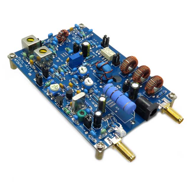
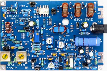
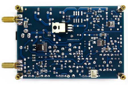
The pictures below show the basic constructed Transverter and the Kit construction notes and overlay diagrams should be carefully followed when constructing. For larger pictures to check orientation of some components click the images below. Construction is quite straight forward with although the bifilar and tri-filar transformers can be a bit tricky to wind correctly. The alignment of the band pass filter and local oscillator are quite easy to do without test equipment.
The pictures below show the basic constructed Transverter and the Kit construction notes and overlay diagrams should be carefully followed when constructing. For larger pictures to check orientation of some components click the images below. Construction is quite straight forward with although the bifilar and tri-filar transformers can be a bit tricky to wind correctly. The alignment of the band pass filter and local oscillator are quite easy to do without test equipment.
It is recommended that the Transverter board is mounted inside an enclosure like the Hammond 1590BBS Die cast enclosure for RF shielding and to provide heatsink cooling for the IRF510 / FQP13N10. The heat-sinking seems ample when the Transverter is used with a 2 minute transmit cycle on WSPR mode with a maximum of 5W output, but it is recommended that a small fan is fitted and run at a lower voltage to keep the board cool to minimize frequency drift due to the Crystal heating. It is suggested that the mounting holes for the board are made before the components are fitted to the board. Some care needs to be made when measuring the holes that need to be drilled, as any inaccuracy could result in the holes on the front of the enclosure being out of alignment. The 6.5mm holes for the SMA connectors may need to be enlarged to 7mm as the board is fitted into the enclosure at an angle as extra clearance may be required.
The Transverter should only be used on an Antenna that is close to 50ohms to avoid damage to the IRF510. To get onto the 472kHz band quickly, an existing Antenna like a 40 or 80m band dipole could be used as a vertical against ground. If the dipole is already fed with coaxial cable then the inner and outer can be connected together, and a series inductance added to resonate the Antenna down on 472kHz. If you have an old switch mode power supply lying around, then the transformer could be used as a series inductance by connecting together windings in series and selecting taps to tune the Antenna closer to resonance. A simple transformer using a FT140-43 core may be required to then match the 50ohm impedance of the Transverter to the feed point. In reality I found that my Antenna was close to 50ohms, but this is probably due to the ground not being very good as it should be much lower than 50ohms. When you are ready to get serious, then a variable inductance ( variometer ) can be constructed which is much more efficient and can be tuned to resonate the Antenna. The trick to it all is to get the vertical part of the antenna as high as possible and away from metal objects like poles, towers, and trees, as it's the vertical part that radiates not the horizontal wires that are capacitance to ground.
Please Note: That the Kit notes are changed at times for improvement or changes to the circuit and have Rev numbers. The PC board also has a Rev number and there was an initial 7 Rev1.1 Kits sold with Rev1.1 boards. All Kits after Rev1.2 are supplied with Rev1.2 boards. Current Kits 2024 are Rev2.x with Rev2.1 PCB's.
1/ The receiver does not receive any signals and appears deaf. D7 may be leaky due to excessively high RF Transmit power being applied to the Transverter. Measure or replace the BAR64-05 D7. Also check the 5 Watt 51R resistor R16 for any damage due to excessive RF power being applied.
2/ With the first initial batch of Rev1.1 Kits using the Rev1.1 board, there appears to be an issue with Transistor T1 failing. The problem never showed up when using digital modes only SSB and was traced to the powersupply switching circuit erratically switching between RX and TX modes with voice when link LK7 is not fitted. This causes high RF power spikes out of band from the PA to bypass the diode switch and appear on the base of T1. The problem can normally be seen when testing on AM mode ( carrier ), and going from TX back to RX mode there is a high spike reading on the S-meter. The solution was to change C40 to a 1uF capacitor so that there is a very small delay that seems to fix the problem. T1 was a NE46134 in the Rev1.1 Kits and is sensitive to failure and can be replaced with a DXT2222A, or PXT2222A, as they are more rugged, or you can use any general purpose transistor that has at least a 40V C-E rating.
3/ TX frequency drift problems in WSPR mode have been directly
traced to heat from the 5W resistor in TX mode heating the PC board
directly under the resistor, and then causing the 78M09 voltage
regulator to slowly decrease in voltage output. This then affects
the crystal oscillator which causes an increase of the 3.2MHz
frequency so a decrease at 472kHz. The 3.2MHz crystals only have a
stability of 30ppm so they will never be great with temperature
changes, but the stability can be improved by keeping the
Transverter as cool as possible with increased ventilation over the
low pass filter and and a small fan mounted over the crystal. Some
small improvements were also seen when the crystal was lifted
slightly off the top of the board, as the ground plane heats and
then directly transfers to the crystal casing. Teflon Crystal
insulators are readily available and are recommended, along with
possibly trying a 40
degree clip on Crystal PTC heater on the crystal. 60
degree clip on Crystal PTC heaters were also tried with
limited success, as standard non oven crystals are really cut for
room temperature and when heated are probably outside the maximum
temperature range. Tests on the other components in the oscillator
showed no drift due to temperature changes, only the crystal was
prone to change with temperature.
4/ Some Rev1.2 Kits were sold in a small number supplied with the FQP13N10 MosFET in place of the IRF510 that appears to produce more RF output power up to 10 Watts, but the gain is way too high and can actually cause the PA and driver to go into oscillation which can cause failure of the GALI-84 driver. Some further investigation is required here, but there was an issue found with instability due to L5 and C22 being close to each other on the board. Current Kits replace C21 and C22 with 1uF 1206 size SMD capacitors that fixes the stability issue or alternatively, fit L5 on the bottom side of the board so that it is a distance from C22. Stability issues will normally show up as a change in RF output power when the lid is fitted onto the enclosure.
5/ In Rev1.3 Kits, the receive amplifier has been modified by replacing T1 with a DXT2222A, R3 with an 56R, and R1 with a 390R which decreases the collector to emitter voltage, and increases the current through T1 to around 40mA which could improve the strong signal handling performance. TR1 if it has failed can be substituted with a DXT2222A, PXT2222A or similar transistor with at least a 40v C-E and 100mA minimum rating. If you get desperate then a BD639 with the flat part mounted against the board with a think smear of heatsink compound is also fine to use.
6.With Kits supplied with the Rev1.2 boards a higher DC voltage can
be fed to the IRF510 to produce more RF output power by
disconnecting Link LK8, and connecting a second DC power supply to
the A5 connector. Currently this has not been tested and it is
expected that the 9:1 Transformer TF2 may need to be changed to a
4:1 for impedance changes with the on the output of the
MosFET. DC to DC step up switching power supply modules that
are rated at 150W are readily available, and can easily supply at
least 3 Amps @ 24vdc. It is up to the individual at their own risk
to possibly damaging the IRF510 if you want to try a higher voltage,
but the MosFET will need substantial Heat-sinking.
7. From Rev1.4 Kits onwards, R15 has been changed from a 680R to a 470R that allows 1W at 3.674MHz to be used instead of 5W. This greatly reduces heating of the circuitry and also frequency drift. This change still allows up to 5W to be used and has been fully tested with a FT817 on 3.674MHz which produced +27dBm low1, +30.5dBm low2, +34dBm low3, +37dBm high.
8. For up to Rev1.5 Kits, the Transverter is not designed to be
hard keyed from a Transceiver and doing so could instantly damage
T1depending on how you connect the keying to the Transverter. A
small delay with C40 1uF is required to slow down the Transverters
TX to RX switching else a very high RF spike from the PA will
destroy T1. The suggestion is to find an output on the back of the
Transceiver that has +12vdc in TX mode, and feed it via a 1k
resistor to the top of LK7. That way when the +12v is disconnected
when going back to RX mode, there is a slow delay going back to RX
mode due to the discharging of C40. If the Transceiver uses an open
collector transistor output that grounds the collector in TX mode,
then you will have to change C42 to a 1uF and connect the
Transceiver via a 1k resistor to C42.
- 472kHz.org: Links to lots of useful information.
- MF Operation at DF0WD:
- VK5FQ Website: Various useful information on Antenna and Transmitters for 136 and 472kHz.
- Short Antenna Tuners for the 136 and 472kHz Bands:
- WG2XKA The Variometer and how to make one:
- G0MRF Variometer Design:
- Antennas By Rudy Severns N6LF:


